
As we all know, the definition of semiconductor is that it has a conductivity between dry conductors and insulators, resistivity between metal and insulator, which is usually at room temperature is within the range of 1mΩ-cm ~ 1GΩ-cm.In recent years, vacuum semiconductor coating in the major semiconductor companies, it is clear that its status is increasingly high, especially in some large-scale integrated system circuit development technology research methods to magnetoelectric conversion devices, light-emitting devices and other development work. Vacuum semiconductor coating has an important role.

Semiconductors are characterized by their intrinsic characteristics, temperature and impurity concentration. Vacuum semiconductor coating materials are distinguished from each other mainly by its constituent compounds. Roughly all are based on boron, carbon, silicon, germanium, arsenic, antimony, tellurium, iodine, etc., and some relatively few GaP, GaAs, lnSb, etc.. There are also some oxide semiconductors, such as FeO, Fe₂O₃, MnO, Cr₂O₃, Cu₂O, etc.
Vacuum evaporation, sputtering coating, ion coating and other equipment can do vacuum semiconductor coating. These coating equipment are all different in their working principle, but they all make the semiconductor material coating material deposited on the substrate, and as the material of the substrate, there is no requirement, it can be a semiconductor or not. In addition, coatings with different electrical and optical properties can be prepared by both impurity diffusion and ion implantation on the surface of the semiconductor substrate in a range. The resulting thin layer can also be processed as a semiconductor coating in general.
Vacuum semiconductor coating is an indispensable presence in electronics whether it is for active or passive devices. With the continuous advancement of vacuum semiconductor coating technology, precise control of film performance has become possible.
In recent years, amorphous coating and polycrystalline coating have made rapid progress in the manufacture of photoconductive devices, coated field-effect tubes, and high-efficiency solar cells. In addition, because of the development of vacuum semiconductor coating and the thin film of sensors, which also substantially reduces the difficulty of material selection and makes the manufacturing process gradually simplified. Vacuum semiconductor coating equipment has become a necessary presence for semiconductor applications. The equipment is widely used for semiconductor coating of camera devices, solar cells, coated transistors, field emission, cathode-light, electron emission, thin film sensing elements, etc.
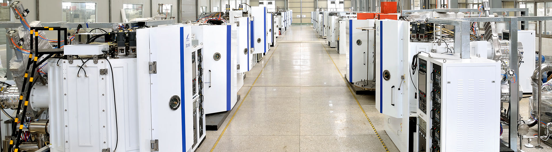
The magnetron sputtering coating line is designed with a fully automatic control system, a convenient and intuitive touch screen human-machine interface. The line is designed with a complete function menu to achieve full monitoring of the operation status for the whole production line components, process parameter setting, operation protection and alarm functions. The whole electrical control system is safe, reliable and stable. Equipped with upper and lower double-sided magnetron sputtering target or single-sided coating system.
The equipment is mainly applied to ceramic circuit boards, chip high-voltage capacitors and other substrate coating, the main application areas are electronic circuit boards.
Post time: Nov-07-2022