
After the discovery of the photovoltaic effect in Europe in 1863, the United States made the first photovoltaic cell with (Se) in 1883. In the early days, photovoltaic cells were mainly used in aerospace, military and other fields. In the past 20 years, the sharp decline in the cost of photovoltaic cells has promoted the widespread application of solar photovoltaic around the world. At the end of 2019, the total installed capacity of solar PV reached 616GW worldwide, and it is expected to reach 50% of the world’s total electricity generation by 2050. Since the absorption of light by photovoltaic semiconductor materials mainly occurs in the thickness range of a few microns to hundreds of microns, and the influence of the surface of semiconductor materials on battery performance is very important, vacuum thin film technology is widely used in solar cell manufacturing.

Industrialized photovoltaic cells are mainly divided into two categories: one is crystalline silicon solar cells, and the other is thin-film solar cells. The latest crystalline silicon cell technologies include passivation emitter and backside cell (PERC) technology, heterojunction cell (HJT) technology, passivation emitter back surface full diffusion (PERT) technology, and oxide-piercing contact (Topcn) cell technology. The functions of thin films in crystalline silicon cells mainly include passivation, anti-reflection, p/n doping, and conductivity. Mainstream thin-film battery technologies include cadmium telluride, copper indium gallium selenide, calcite and other technologies. The film is mainly used as a light absorbing layer, conductive layer, etc. Various vacuum thin film technologies are used in the preparation of thin films in photovoltaic cells.
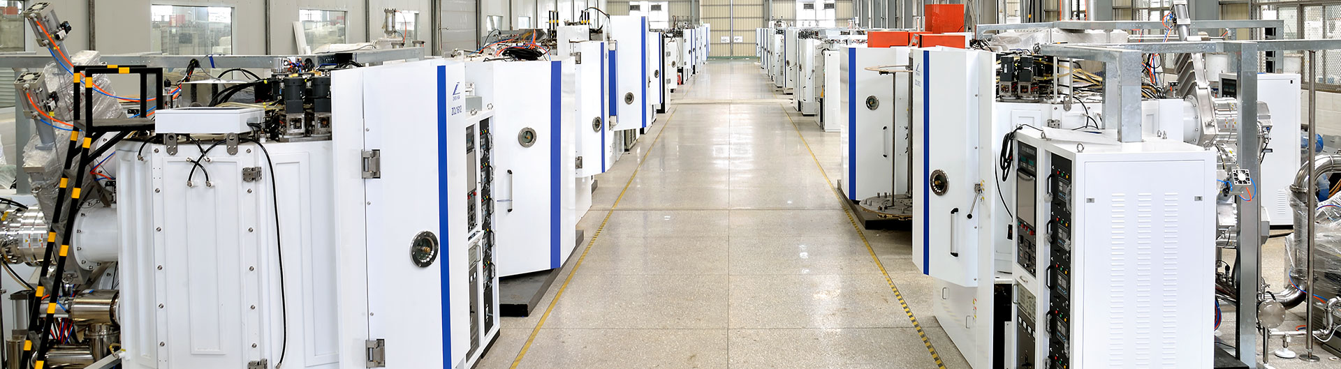
Zhenhua solar photovoltaic coating production line introduction:
Equipment features:
1. Adopt modular structure, which can increase the chamber according to the needs of work and efficiency, which is convenient and flexible;
2. The production process can be fully monitored, and the process parameters can be traced, which is convenient to track production;
4. The material rack can automatically returned, and the use of the manipulator can connect the former and latter processes, reduce labor costs, high degree of automation, high efficiency and saving energy.
It is suitable for Ti, Cu, Al, Cr, Ni, Ag, Sn and other elemental metals, and has been widely used in semiconductor electronic components, such as: ceramic substrates, ceramic capacitors, LED ceramic brackets, etc.
Post time: Apr-07-2023