
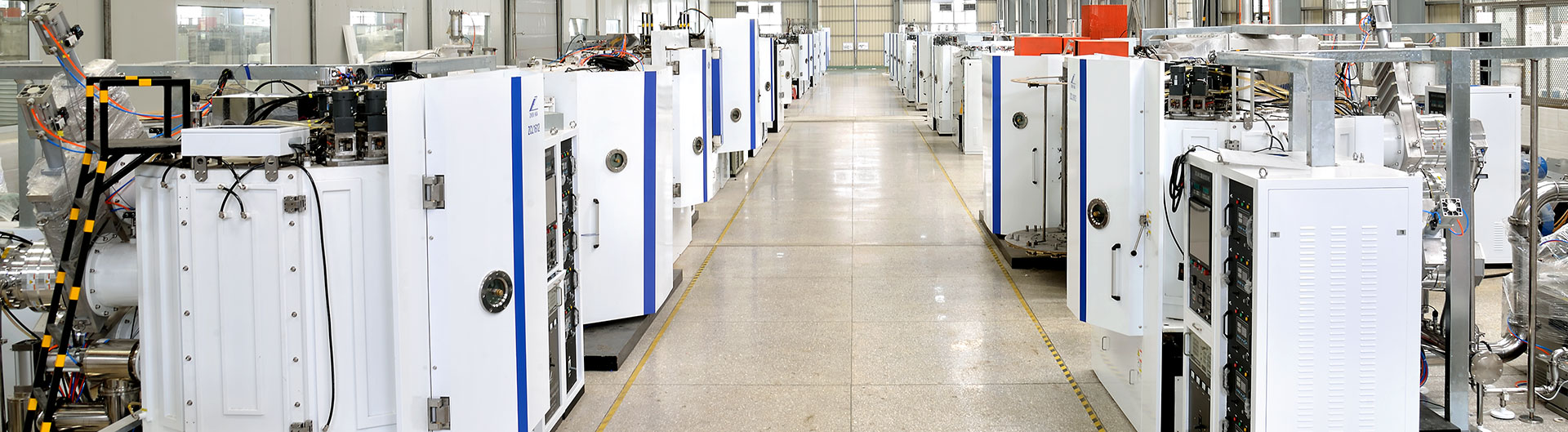
In materials science and engineering, the field of thin film coatings plays a vital role in industries ranging from electronics to advanced manufacturing. Among the different technologies available, physical vapor deposition (PVD) sputtering has emerged as an innovative and efficient method for depositing thin films on substrates. This article will delve into the world of PVD sputtering, discussing its applications, benefits and latest developments.
PVD sputtering, also known as magnetron sputtering, is a technique widely used in the semiconductor industry to deposit thin films on wafers. It involves using plasma to remove atoms from a target material, which is then deposited onto a substrate, forming a thin film. The process offers many advantages, such as precise control of film thickness, excellent adhesion, and the ability to deposit a variety of materials including metals, oxides, and nitrides.
The applications of PVD sputtering are wide and varied. In the electronics industry, it is commonly used to deposit conductive materials such as aluminum and copper, enabling the production of tiny components and integrated circuits. In addition, PVD sputtering is widely used in the optical coating industry, such as anti-reflective coatings on lenses and mirrors to enhance light transmission performance.
Recent advances in PVD sputtering technology are making it more and more popular. A notable development is the introduction of reactive sputtering, which can deposit thin films of compounds with enhanced properties. By introducing reactive gases into the vacuum chamber during deposition, manufacturers can control the composition and stoichiometry of the deposited films, providing improved performance and functionality.
Additionally, target innovations have expanded the capabilities of PVD sputtering. For example, using composite targets comprising multiple materials can deposit highly specialized thin films with unique properties. This opens the door to the development of new materials for advanced electronics, energy storage and biomedical devices.
In summary, PVD sputtering is a powerful thin film coating technique with a wide range of applications and recent advances. With precise control over thin film deposition and compatibility with various materials, it has become a staple in industries such as electronics and optics. Ongoing research and innovation in the field of PVD sputtering is expected to further enhance its capabilities, enabling the creation of new materials and pushing the boundaries of technological advancement.
Post time: Jul-24-2023