
In today’s digital revolution, the explosive growth of data transmission is being driven by high-frequency interactions in smartphones, immersive AR/VR experiences, and massive computing workloads in high-performance computing. Traditional 2D packaging—with long interconnect paths and high transmission losses—can no longer break through performance bottlenecks.
As a result, chip stacking and 3D packaging have emerged as the industry’s strategic direction. To enable truly efficient 3D interconnections, Through Glass Via (TGV) technology has stood out with its unique advantages, moving from R&D reserves into industrial application. TGV is now becoming a key enabler for next-generation electronic devices.
1. TGV Technology: The “Bridge” of 3D Interconnection
1.1 Core Concept: What Exactly is TGV?
The essence of TGV is the fabrication of vertical microvias through a glass substrate. These vias act as electrical bridges, directly connecting stacked chips or components, enabling both signal and power transmission. Compared with traditional “planar wiring,” vertical interconnection dramatically shortens transmission paths and underpins device miniaturization and high integration.
1.2 Why Glass Substrates Are the Natural Carrier for TGV
TGV surpasses TSV (Through Silicon Via) due to three key material advantages of glass:
Low dielectric constant – safeguarding high-frequency signals: Glass inherently features a low dielectric constant, minimizing dielectric loss during transmission and preserving signal integrity in high-frequency applications such as 5G and HPC.
Thermal expansion compatibility with silicon – enhancing reliability: Glass closely matches silicon’s coefficient of thermal expansion, reducing thermo-mechanical stress and failures during thermal cycling, thereby extending device lifetime.
High optical transparency – enabling optoelectronic integration: Unlike opaque silicon, glass transparency supports electro-optical hybrid applications. For instance, in silicon photonics modules, glass enables both electrical interconnects and optical signal transmission; in AR/VR microdisplays, transparency minimizes optical blockage and improves brightness and clarity.
1.3 From TSV to TGV: A Natural Evolution
Before TGV, TSV was the dominant 3D interconnect technology. However, TSV faces mounting challenges as integration density rises:
High cost: Complex process flows—etching, insulation, metallization—make TSV less suitable for large-scale manufacturing.
Reliability concerns: Thermal expansion mismatch between silicon and other materials often leads to cracking or solder joint failure.
Limited application scope: Silicon’s opacity excludes TSV from optoelectronic applications requiring transparency.
TGV effectively addresses these pain points, making it the preferred next-generation interconnect solution.
2. Via Coating: The Core Enabler That Makes TGV Functional
2.1 Key Insight: Without Coating, a TGV is Just an “Empty Tube”
Glass vias are inherently insulating and cannot conduct electricity. To enable interconnection, a conformal conductive layer (usually a metal film) must be deposited along the via sidewalls. This layer functions as a signal highway—determining speed, loss, and stability. Non-uniform or defective coatings cause higher resistance, signal attenuation, or even open circuits, making via metallization the lifeline of TGV technology.
2.2 The Challenges: Two Critical Pain Points
High Aspect Ratio Coverage
TGV diameters are now in the micrometer range (down to ~30 μm) with depths exceeding 10:1 aspect ratios. Traditional deposition methods struggle to achieve bottom coverage and uniform sidewall films, often leaving uncoated “dead zones” that degrade interconnect performance.
Defect Control – The Hidden Killer
Corners and rough via sidewalls are prone to deposition voids or bubbles. These defects cause localized resistance spikes or open circuits, directly breaking connections between chips and devices. Defect suppression is thus the central challenge of TGV coating.
3. Four Coating Routes: Strengths and Limitations
Physical Vapor Deposition (PVD): Mature but Limited
Processes like evaporation and sputtering provide high-purity, strongly adherent films. However, due to its “line-of-sight” nature, PVD struggles with high aspect ratio vias and is best suited for vias below ~5:1 aspect ratios.
Chemical Vapor Deposition (CVD): High Aspect Ratio Capable but Costly
CVD uses gaseous precursors that diffuse along via sidewalls, yielding uniform coatings even in high aspect ratio structures. However, high temperature and pressure conditions risk damaging glass substrates, and equipment cost is high, making it suitable mainly for high-end applications.
Electrochemical Deposition (ECD): Cost-Effective Mass Production
ECD plates conductive films by reducing metal ions on via sidewalls. It offers low cost and high throughput, ideal for volume production. However, tight control of electrolyte concentration and current density is essential—deviations lead to porous films or contamination. It is typically applied to vias 5–50 μm in diameter.
Atomic Layer Deposition (ALD): The Precision Solution
ALD achieves atomic-scale thickness control and excellent conformality, making it ideal for very high aspect ratio vias. It solves the coverage challenge but suffers from extremely slow deposition rates and high cost. Thus, ALD is mainly reserved for aerospace and high-reliability sensors.
4. The Value of TGV Coating: Driving 3D Interconnection Performance
Speed Breakthrough – High-Speed Direct Connections
In 2D packaging, signals must travel long distances, increasing loss. With TGV metallization, chip-to-board and chip-to-system interconnects become short, vertical, and low-loss. In HPC servers, TGV-coated vias enable CPU-to-memory/GPU communication speeds to improve by over 30%, reducing latency and boosting system efficiency.
Energy Efficiency – Lower Delay and Power Consumption
Shorter interconnect paths reduce delay, while low-resistance coatings minimize Joule heating. For example, TGV-enabled smartphone chip packaging can reduce core power consumption by 15–20%, extending battery life and improving user experience.
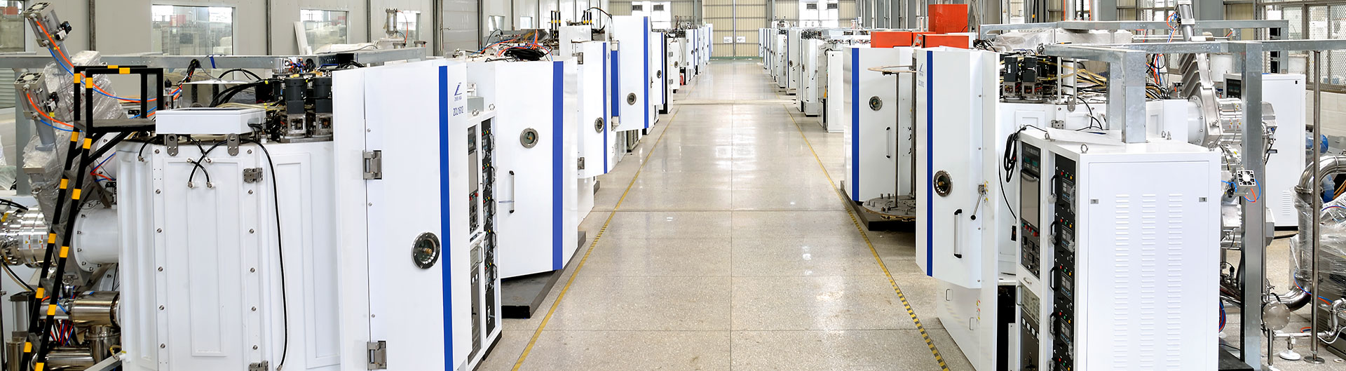
5. Zhenhua Vacuum: Advanced TGV Coating Solutions
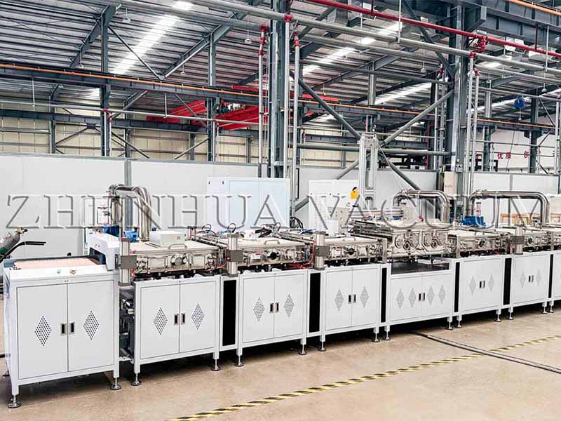
Equipment Advantages
Deep-Via Optimization
Proprietary deep-hole coating technology enables uniform seed layer deposition even in vias as small as 30 μm with aspect ratios beyond 10:1—solving one of the industry’s toughest challenges.
Customizable Substrate Handling
Supports a range of glass substrate sizes, including 600 × 600 mm / 510 × 515 mm, with scalability to larger formats.
Process Flexibility – Multi-Material Compatibility
Supports conductive and functional films such as Cu, Ti, W, Ni, and Pt, meeting diverse application requirements for conductivity and corrosion resistance.
Stable Performance and Easy Maintenance
Equipped with intelligent process control systems for real-time monitoring of film thickness uniformity, and a modular design for easy maintenance and reduced downtime.
Application Scope
Applicable to TGV/TSV/TMV advanced packaging, enabling conformal seed layer deposition in deep vias with aspect ratios of 10:1.
—This article was published by vacuum coating equipment manufacturer Zhenhua Vacuum
Post time: Sep-27-2025