
As semiconductor devices continue to scale down while integrating more functionalities, packaging technologies face unprecedented challenges. Vacuum coating has emerged as a key enabling process in advanced semiconductor packaging, ensuring device miniaturization, higher performance, and long-term reliability. By leveraging thin-film engineering techniques such as physical vapor deposition (PVD), chemical vapor deposition (CVD), and atomic layer deposition (ALD), manufacturers can address critical demands for barrier protection, electrical performance, and thermal management in next-generation chips.
Common Challenges in Semiconductor Packaging
Semiconductor packaging is no longer a simple protective step but a performance-critical stage. Typical challenges include:
Moisture and Oxygen Ingress
Encapsulated devices are highly sensitive to environmental exposure. Even trace levels of moisture or oxygen diffusion can lead to corrosion, metal migration, or dielectric degradation.
Barrier Layer Reliability
Conventional polymer encapsulants often exhibit insufficient barrier properties. Without robust thin-film coatings, chips are prone to reliability failures in high-humidity or high-temperature conditions.
Electromigration and Interconnect Stability
High current densities in advanced nodes accelerate electromigration. Poor adhesion or non-uniform coatings can compromise interconnect lifetime.
Thermal Dissipation Limitations
As device power density rises, inadequate thermal management coatings can lead to localized hotspots, performance degradation, and shortened device lifespans.
Miniaturization and Aspect Ratio Coverage
Advanced packaging structures such as Through-Silicon Vias (TSVs) and Through-Glass Vias (TGVs) demand conformal coatings inside high aspect ratio trenches and vias, which remain a key technical bottleneck.
Vacuum Coating Solutions
1. Moisture/Oxygen Barrier Coatings
SiO₂, SiNₓ, and Al₂O₃ thin films deposited via PVD or ALD serve as hermetic encapsulation layers, significantly reducing water vapor transmission rates (WVTR).
Multi-layer barrier stacks combining inorganic and hybrid layers achieve superior reliability, critical for RF modules and MEMS packaging.
2. Adhesion-Promoting and Interface Layers
Ti, Cr, or TiN adhesion layers enhance the bonding strength between metallization layers and dielectrics, preventing delamination during thermal cycling.
Plasma surface treatments further improve wetting and film nucleation on low-surface-energy substrates.
3. Diffusion and Electromigration Suppression Layers
Ta, TaN, and Ru barrier layers deposited via magnetron sputtering act as effective diffusion barriers in Cu interconnects.
These layers mitigate electromigration, preserving interconnect conductivity under high current stress.
4. Thermal Management Coatings
High thermal conductivity coatings such as diamond-like carbon (DLC) or AlN films enhance heat dissipation.
Tailored coatings enable integration into power semiconductor modules, SiC/GaN devices, and high-performance computing (HPC) chips.
5. Conformal Coatings for High Aspect Ratio Structures
ALD provides atomic-level control, ensuring conformal and pinhole-free films in TSVs and TGVs with aspect ratios exceeding 10:1.
This is crucial for 3D IC packaging, where interconnect density and reliability directly affect yield.
Case Applications
MEMS Packaging: Thin-film encapsulation with Al₂O₃/SiNₓ stacks improves hermeticity, extending device lifetime in automotive and industrial environments.
RF Front-End Modules: Multi-layer barrier coatings reduce parasitic capacitance and moisture-induced performance drift.
Power Electronics: DLC thermal spreader coatings enhance heat dissipation in SiC-based MOSFETs, enabling higher operating efficiency.
3D Integration: Conformal ALD coatings in TSV/TGV ensure reliable via insulation and metallization for high-bandwidth memory (HBM) devices.
Advantages of Vacuum Coating in Packaging
High Reliability: Superior barrier and adhesion performance ensures long-term device stability.
Scalability: Vacuum-based deposition systems support wafer-level packaging (WLP) and panel-level packaging (PLP), enabling cost-effective mass production.
Process Flexibility: Compatible with diverse materials (Si, GaAs, SiC, glass, polymers), meeting heterogeneous integration needs.
Environmental Compliance: Eliminates high-pollution wet processes such as electroplating, aligning with green manufacturing standards.
Conclusion
Vacuum coating has become a cornerstone of advanced semiconductor packaging, addressing challenges in barrier protection, thermal management, and high-aspect-ratio coverage. As the industry transitions to heterogeneous integration, chiplet architectures, and 3D stacking, the demand for precision thin-film deposition will only intensify.
Through continuous innovation in PVD, ALD, and hybrid coating platforms, vacuum coating solutions are not just enhancing reliability but actively enabling the future of semiconductor packaging.
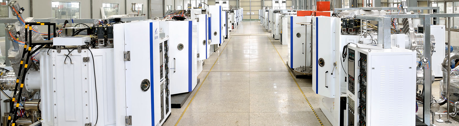
—This article was published by vacuum coating equipment manufacturer Zhenhua Vacuum
Post time: Sep-27-2025