
As technology continues to advance, it’s no surprise that the semiconductor industry plays a vital role in shaping the world around us. Among the many transformative technologies in the industry, PVD (Physical Vapor Deposition) stands out as a game changer.
PVD is a cutting-edge technology used to deposit thin films on a variety of surfaces, primarily in semiconductor manufacturing. What makes PVD so compelling is its ability to produce high-quality, uniform films that ensure precise performance and reliability of semiconductor devices.
The semiconductor PVD process involves evaporating or sputtering materials onto a substrate. By carefully controlling temperature, pressure and deposition time, manufacturers can achieve dramatic results. This technology enables greater flexibility in material selection, resulting in improved semiconductor device performance and novel functionality.
The rapid growth of the semiconductor industry is driven in large part by the growing demand for smaller, faster, and more efficient electronic devices. PVD technology has become an important tool to meet these needs. Semiconductor PVD plays a vital role in the manufacturing of advanced microchips and other electronic components by enabling precise deposition of ultra-thin films.
The consumer electronics sector is one of the areas that has benefited greatly from advances in semiconductor PVD. From smartphones to laptops, we rely on these devices to complete a variety of daily tasks. The integration of PVD technology in manufacturing ensures improved device performance, extended battery life, and an overall better user experience.
In addition, the automotive industry is not far behind in embracing semiconductor PVD. With the rise of electric vehicles and advanced driver assistance systems, PVD is helping to bring innovative solutions to the forefront. From the deposition of conductive films for touch screens to the enhancement of energy storage capabilities, semiconductor PVD is revolutionizing the driving experience.
The medical field is another beneficiary of semiconductor PVD. Medical devices such as biosensors and implantable devices require precise and reliable performance. PVD creates biocompatible coatings and microstructures that enhance the functionality and durability of these critical devices, ultimately improving patient care and outcomes.
As the demand for high-performance and energy-saving equipment continues to grow, so does the need for continued advancements in semiconductor PVD technology. Researchers and engineers are exploring new materials and technologies to further enhance the capabilities of PVD. These efforts aim to overcome existing limitations and pave the way for more breakthroughs in the semiconductor industry.
In conclusion, semiconductor PVD has undoubtedly transformed the technology industry. Its ability to deposit thin films with exceptional precision and reliability has enabled the development of smaller, faster, and more efficient electronic devices. From consumer electronics to automotive and medical applications, PVD technology is driving innovation and improving every aspect of our lives. Looking ahead, continued advances in semiconductor PVD hold great promise for further changes in the industry and pushing the boundaries of what is possible.
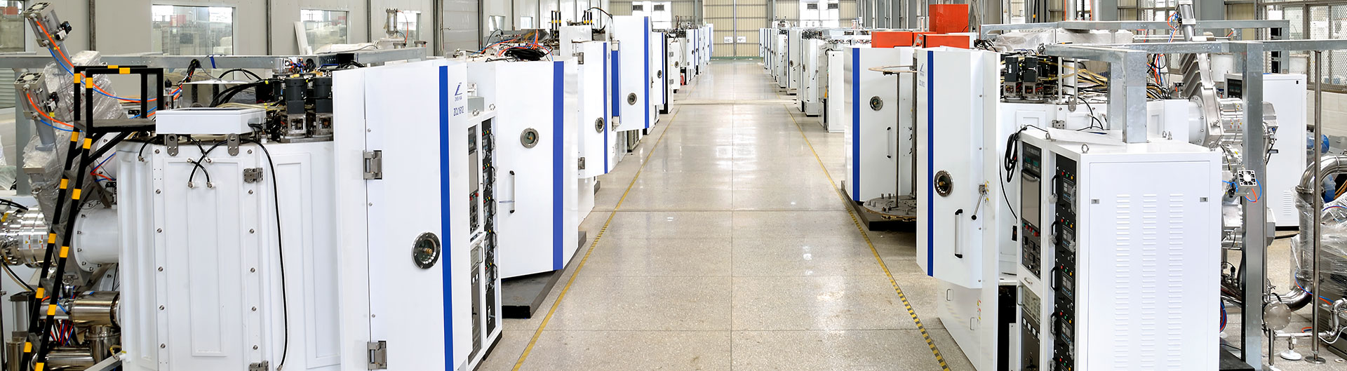
——This article is released by vacuum coating machine manufacturer Guangdong Zhenhua
Post time: Sep-21-2023