
In the evolution of semiconductor packaging technology, vertical interconnects have always been a key factor determining system performance, footprint, and power consumption. From early wire bonding and flip-chip techniques to the emergence of 3D stacked ICs, the industry has been seeking higher density and shorter interconnect solutions.
In this context, TSV (Through Silicon Via) and TGV (Through Glass Via) have emerged as two mainstream vertical interconnect technologies. They differ in material systems, manufacturing processes, performance characteristics, and application domains, representing a pivotal point in next-generation packaging development.
I. TSV: Pioneer of 3D Packaging
1. Technical Principle
TSV refers to high-aspect-ratio vias etched through a silicon substrate (typically tens to hundreds of microns deep), followed by the formation of an insulating layer, metal seed layer, and metal fill (usually copper) on the via walls. These vertical vias enable high-speed electrical interconnections between stacked chip layers.
2. Process Flow
The typical TSV fabrication process includes:
Deep Silicon Etching (DRIE): Create high-aspect-ratio vias in the silicon wafer.
Insulating Layer Deposition: Usually PECVD-deposited SiO₂ to electrically isolate the metal fill from the silicon substrate.
Seed Layer Deposition and Electroplating: PVD deposition of a metal seed layer followed by copper electroplating.
Chemical Mechanical Polishing (CMP): Remove excess metal to achieve a planarized surface.
3. Advantages and Limitations
TSV offers extremely short interconnect paths, low signal latency, low power consumption, and high bandwidth, making it a critical enabler for high-performance computing and high-bandwidth memory.
However, TSV also has limitations:
Thermal stress issues: Large mismatch in CTE between silicon and copper can reduce reliability.
High process cost: Deep etching, electroplating, and CMP are complex and yield-sensitive.
Electrical insulation challenges: Thickness and uniformity of the insulating layer directly affect dielectric strength.
As chip integration density increases, conflicts between yield and cost have driven the exploration of alternative materials—creating the opportunity for TGV.
II. TGV: Glass-Based Interconnect Innovation
1. Technical Principle
TGV uses glass substrates instead of silicon. High-precision vias are formed by laser drilling or wet etching, followed by deposition of a metal seed layer and electroplating, achieving vertical interconnects similar to TSV.
Glass offers excellent electrical insulation, low dielectric constant (Dk), low dielectric loss (Df), and outstanding dimensional stability, making TGV highly attractive for high-speed signal transmission and optoelectronic packaging.
2. Process Flow
Key steps in TGV fabrication include:
Laser Drilling: Ultrafast lasers form microvias in glass with diameters typically ranging from 20–150 μm.
Seed Layer Deposition: PVD, such as magnetron sputtering, deposits a uniform conductive layer on the via walls.
Metal Electroplating: Copper or nickel-copper alloy fills the vias to form through-glass electrical connections.
Planarization and Patterning: Enables multi-layer interconnects or bonding to IC chips.
3. Advantages
Compared with TSV, TGV demonstrates several benefits:
Low dielectric loss: Glass Dk is about 1/3 of silicon, reducing signal crosstalk and insertion loss.
Excellent thermal stability: CTE close to metals, minimizing thermal stress.
Optical transparency: Supports optoelectronic integration in photonics and sensors.
Controllable cost: Laser drilling and glass processing are maturing, suitable for large-area panel-level production.
III. TSV vs TGV: Comparison and Application Domains
| Item | TSV (Through Silicon Via) | TGV (Through Glass Via) |
| Substrate | Monocrystalline silicon | Specialty glass (Borofloat, Corning, Schott, etc.) |
| Diameter of hole | 5–50 μm | 20–150 μm |
| Hole Depth | 30–100 μm | 100–400 μm |
| Insulation | Additional insulating layer required | Glass intrinsically insulating |
| Thermal Expansion Coefficient Matching | Significant differences compared with Cu | Similar to Cu, low thermal stress |
| Process Cost | High | Relatively lower |
| Applications | Logic/Memory 3D Stacking | SiP, sensors, optoelectronic packaging, antennas, MEMS |
TSV remains the mainstream choice for high-performance logic and memory 3D stacking, while TGV is rapidly expanding in SiP, optoelectronic integration, sensors, and RF devices.
With glass substrate sizes reaching panel-level packaging (PLP), TGV is becoming an ideal interconnect platform for 5G communication, automotive radar, AR optics, and Mini/Micro LED packaging.
IV. From Silicon to Glass: System-Level Benefits
The introduction of glass is not merely a material replacement; it represents a shift in system-level design philosophy.
Electrical performance: Low Dk glass significantly reduces signal delay and power consumption.
Structural integrity: TGV offers higher planarity and lower warpage for large-area packaging.
Manufacturing flexibility: Laser processing combined with vacuum PVD allows high process compatibility and scalability.
In particular, for optoelectronic integration, the optical transparency of glass enables packaging designs where the substrate supports not only electrical interconnects but also waveguides, lenses, and sensor windows, which is difficult to achieve with TSV.
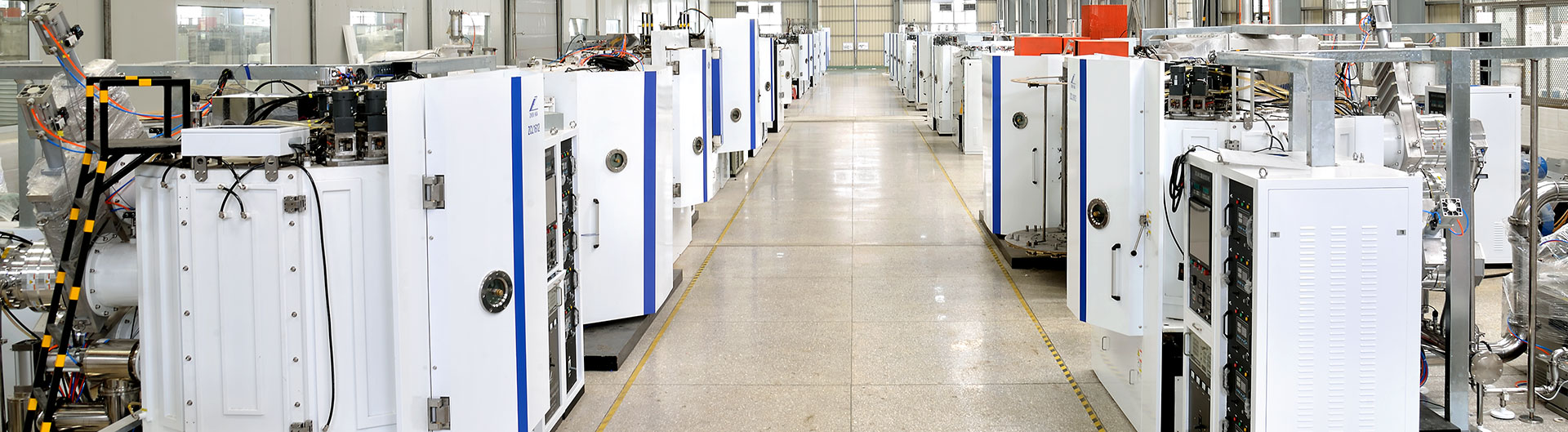
V. ZhenHua Vacuum TGV Seed Layer Coating Solution
Equipment Advantages:
Deep Via Coating Optimization: Proprietary deep via coating technology capable of handling vias as small as 30 μm with >10:1 aspect ratio, addressing complex deep via challenges.
Customizable for Various Sizes: Supports glass substrates including 600×600 mm, 510×515 mm, or larger.
Process Flexibility: Compatible with Cu, Ti, Ni, Pt, and other conductive or functional thin films to meet diverse electrical and corrosion resistance requirements.
Stable Performance & Easy Maintenance: Equipped with smart control for automatic parameter adjustment and real-time monitoring of thickness uniformity; modular design facilitates maintenance and reduces downtime.
Application Scope: Suitable for TGV/TSV/TMV advanced packaging, achieving deep via seed layer coating with 10:1 aspect ratio.
—This article was published by vacuum coating equipment manufacturer Zhenhua Vacuum
Post time: Oct-16-2025