
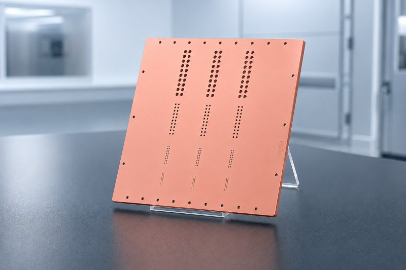
As chips and electronic devices continue to evolve toward miniaturization and higher integration, circuit fabrication solely on the surface of ceramic substrates can no longer meet increasingly demanding interconnection and routing requirements. Microvias are therefore required to electrically connect the front and back sides of the substrate, shortening interconnect paths and increasing circuit density. As a result, DPC (Direct Plated Copper) via metallization technology has been widely adopted in applications including LEDs, lasers, optical communications, RF devices, and power electronics.
However, ceramic substrates are inherently electrically insulating. Simply forming microvias through the substrate does not establish electrical continuity between the two sides. The real challenge is to form a continuous and reliable metallic seed layer along the inner walls of the microvias.
1. How Is Electrical Continuity Established Through Ceramic Microvias?
DPC via metallization typically begins with laser drilling to form microvias in the ceramic substrate, generally in the form of tapered or straight-through holes. The microvias and substrate surface are then thoroughly cleaned and degassed to remove drilling residues, moisture, and other contaminants. A vacuum sputtering process is subsequently used to deposit a Ti adhesion layer, typically 50–200 nm thick, followed by a Cu conductive seed layer, typically 0.5–2 μm thick, on the substrate surface and along the inner walls of the microvias.
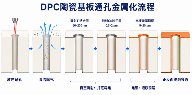
The Ti layer serves as an adhesion layer to improve the bonding strength between the metal film and ceramic substrate, while the Cu seed layer provides a continuous conductive foundation for subsequent electroplating. The copper layer is then further built up by electroplating, typically to a thickness of 5–20 μm, ultimately establishing reliable electrical continuity between the circuits on the front and back sides through the metallized vias. In simple terms, vacuum sputtering provides the conductive foundation, while subsequent electroplating builds up the copper thickness, thereby reducing via resistance and improving interconnection reliability.
Although the process appears straightforward, reliable via interconnection depends on one critical prerequisite: the Ti/Cu seed layer must completely and continuously cover the substrate surface and the entire inner wall of each microvia.
2. Four Key Challenges of Vacuum Sputtering Ti/Cu Seed Layers for DPC Vias
Forming a continuous seed layer inside narrow microvias is far from straightforward. Residues remaining inside the vias can compromise film adhesion, while the microvia geometry makes sidewall coverage increasingly difficult. Local discontinuities in the seed layer can interrupt subsequent electroplating, while variations between different substrate locations and production batches can affect overall process stability. The key challenges of vacuum sputtering for DPC via metallization can be summarized in four areas.
1. Residues Inside the Vias Can Compromise Film Adhesion
After laser drilling, ceramic substrates may contain ceramic particles, recast material, drilling debris, and adsorbed moisture inside the microvias. For microvias with small diameters and high aspect ratios, these residues are often much more difficult to remove than surface contamination. If cleaning and degassing are insufficient, the Ti adhesion layer may not form a strong and reliable bond with the ceramic sidewall. Such defects may not become immediately apparent after coating, but can gradually develop into blistering and delamination during subsequent electroplating, soldering, or high-temperature operation.
2. Higher Aspect Ratios Make Sidewall Coverage More Difficult
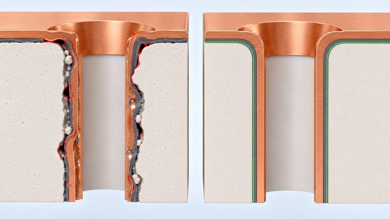
The sputtering difficulty of a microvia cannot be evaluated solely by its depth; the ratio between via depth and via diameter—the aspect ratio—is equally important. For example, a via with a diameter of 60 μm and a depth of 300 μm has an aspect ratio of 5:1. As the aspect ratio increases, the via entrance creates greater geometric shadowing of sputtered particles, reducing the number of particles that can reach the middle section of the sidewall. This can result in relatively thick films on the substrate surface and near the via opening, while the middle section of the via sidewall becomes significantly thinner or even discontinuous.
3. An Incomplete Seed Layer Can Prevent Reliable Via Interconnection
The fundamental requirement of DPC via metallization is not simply whether copper is present on the via wall, but whether the Ti/Cu seed layer can extend continuously from the front side of the substrate, along the entire via sidewall, to the back side. Even a small discontinuity in the seed layer can interrupt the conductive path required for subsequent electroplating. Therefore, seed-layer quality cannot be evaluated solely by surface appearance or average film thickness. Particular attention must be paid to the thinnest section of the via sidewall and whether continuous electrical conductivity is maintained throughout the metallized path.
4. Passing a Single Sample Does Not Guarantee Batch-to-Batch Stability
Achieving the required surface film thickness on a single sample does not necessarily mean that the process is ready for mass production. DPC manufacturing also requires tight control of coating uniformity between the front and back surfaces, between the center and edge regions of the substrate, across different fixture positions, and from batch to batch. For ceramic substrates containing a large number of microvias, process evaluation should not focus solely on average film thickness. More importantly, the thinnest region of the via sidewall must consistently maintain the electrical conductivity required for subsequent electroplating.
3. What Happens When the Seed Layer Is Not Properly Deposited?
The Ti/Cu seed layer provides the conductive foundation required for subsequent electroplating. If the seed layer on the via sidewall is too thin, incompletely covered, or contains discontinuities, the electroplating current cannot be transferred continuously along the sidewall, and copper ions cannot be properly reduced and deposited at the defective locations. As electroplating proceeds and the copper layer builds up, initially minor areas of insufficient coverage can develop into copper-layer voids, localized thickness deficiencies, or discontinuous plating within the via.
These defects directly affect the interconnection quality of the circuits on the front and back sides of the ceramic substrate. In less severe cases, they can result in increased via resistance, localized heat generation, and fluctuations in electrical performance. In more serious cases, the circuits on the two sides may fail to achieve electrical continuity. During subsequent soldering, high-temperature aging, or thermal cycling, defective areas may further develop blistering, delamination, or circuit cracking, reducing product yield and long-term reliability and potentially resulting in device failure.
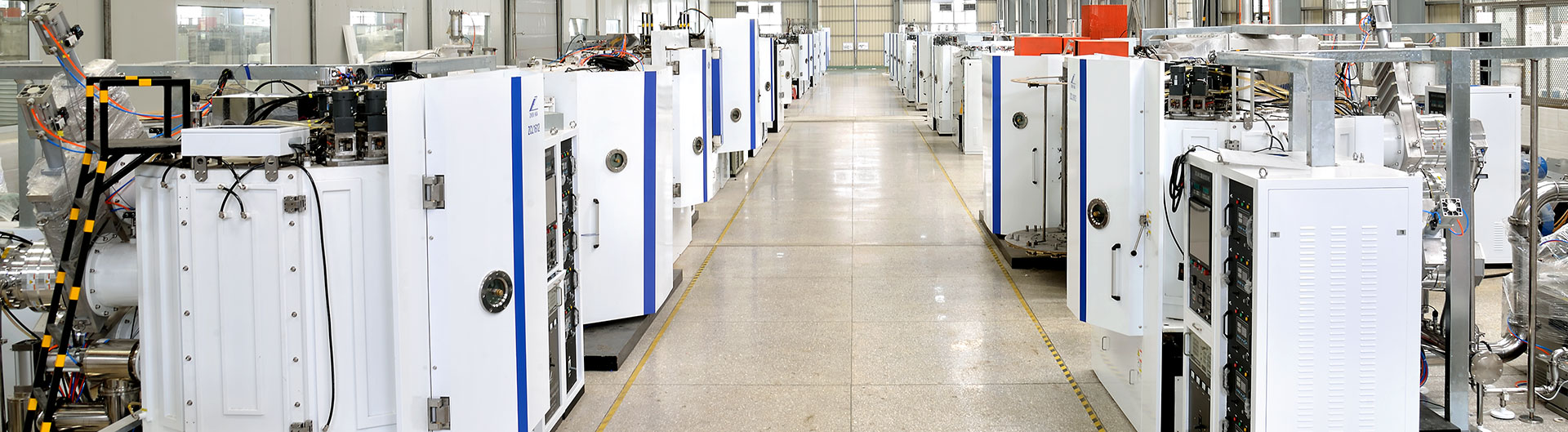
4. Zhenhua Vacuum’s Mass-Production Solution for Ceramic Substrate Via Metallization — DPC Ceramic Substrate Vacuum Coating Production Line
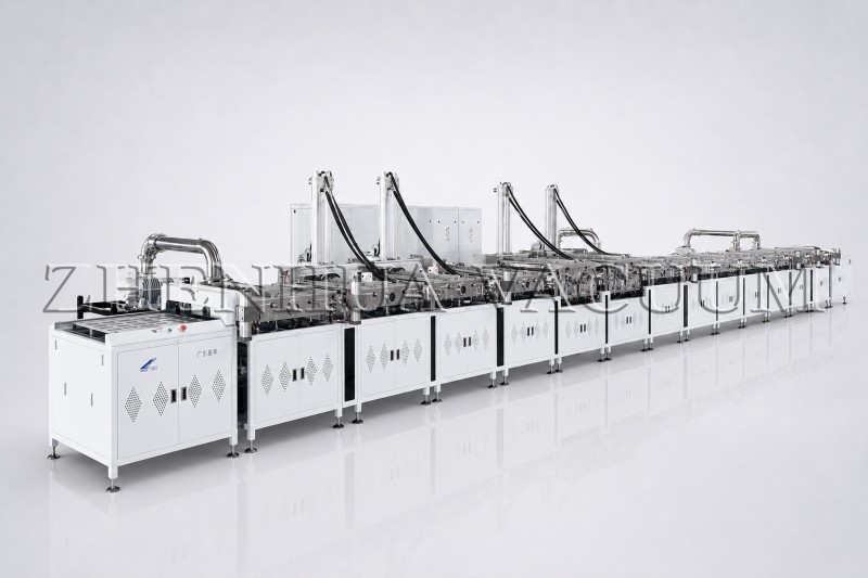
Equipment Advantages:
Automation: A fully automated coating and workpiece-carrier transfer system reduces manual intervention while improving production efficiency and shortening overall cycle time.
Throughput: Supports 120 mm × 120 mm substrates with a production capacity of up to 288 pcs per hour.
Performance: Improves electrical conductivity while enhancing the heat dissipation performance of the ceramic substrate.
Via Metallization: An optimized magnetic-field configuration enables efficient and uniform coating coverage within microvias.
Process: Supports double-sided coating to improve overall film-thickness uniformity and coating consistency.
Applications:
The equipment can deposit a variety of elemental metal films, including Ti, Cu, Al, Sn, Cr, Ag, and Ni, and has been widely applied in the semiconductor and electronic component industries for applications such as ceramic substrates, ceramic capacitors, and LED ceramic packages/supports.
5. Conclusion
Zhenhua Vacuum focuses on the front-end vacuum sputtering process for DPC manufacturing. By enhancing microvia sidewall coverage and combining double-sided coating technology with automated production, the solution provides stable Ti/Cu seed layers for subsequent electroplating and reliable via interconnection. This helps customers achieve consistent mass production while supporting the broader adoption of DPC ceramic substrates in semiconductor and advanced electronic applications.
-This article was published by vacuum coating equipment manufacturer Zhenhua Vacuum
Post time: Aug-27-2026